
Preparation and Properties of Niobium Nitride Thin Films by Reduction Nitridation Method
Nb4N5 thin films were prepared using niobium pentachloride as raw material by ammonia reduction nitridation method. The composition, morphology, and surface enhanced Raman spectroscopic properties of the thin films were investigated using XRD, SEM, UV-VIS-NIR, and RAMAN measurements. The results show that the Nb4N5 film has a high degree of crystallization, a relatively pure phase, and no other impurities. The film has fewer surface cracks, a particle size of 40 nm, and a film thickness of 210 nm. The synthesized Nb4N5 film has a plasmon resonance absorption peak at 300 to 500 nm in its absorption spectrum, an infrared region reflectance of more than 30%, and a square resistance of 552 Ω/□. The film has good SERS activity.
Keywords niobium nitride; film; Ammonia reduction nitridation method
0 Introduction
Niobium nitride is a transition metal nitride of the fifth group. It has a high melting point and hardness, excellent mechanical properties, thermal stability, and chemical stability, and excellent superconducting properties. It is widely used in wear-resistant coatings, building energy conservation, fire-resistant plasma effects, supercapacitors, and other fields. It can also be used to make superconducting quantum devices. In addition, niobium nitride exhibits surface plasmon resonance (SPR) effects, which indicate that electromagnetic fields near the surface of the material are enhanced. Therefore, this material may have surface enhanced Raman scattering (SERS) properties through electromagnetic field enhancement effects.
Currently, the preparation methods of niobium nitride thin films include physical vapor deposition and plasma chemical vapor deposition. However, the above preparation methods require expensive equipment and complex process flow. In contrast, the sol gel reduction nitridation method can more easily prepare nitride films on the substrate. Its reaction process is simple, the film composition is easy to control, the film and substrate bonding strength is high, and the preparation cost is low. However, there are few reports on using this method to prepare niobium nitride thin films. Therefore, in this paper, Nb2O5 thin films were first prepared by sol-gel method, and then reduced and nitrided in ammonia to successfully prepare Nb4N5 thin films, and their properties were studied.
Experiment
1.1 Experimental methods
Raw materials: niobium chloride (NbCl5, AR), auxiliary polyvinyl pyrrolidone (PVP, Mw=1300 000, AR), solvents: anhydrous ethanol (EtOH, AR) and N, N-dimethylformamide (DMF, AR), all purchased from Aladdin Chemical Co., Ltd.
A starting solution was prepared by mixing 0.614 5 g of niobium chloride with 9 ml of anhydrous ethanol, then adding 0.50 g of PVP as an adhesive, and 1.25 ml of DMF as a dispersant. The precursor solution was magnetically stirred for 2 hours until it became clear and completely dissolved.
Place the quartz glass in ultrasound and wash with water and ethanol for 15 minutes. Deposition was carried out on a quartz glass substrate, and the starting solution was rotationally coated for 20 seconds at 3500 rpm. Then, the Nb2O5 thin film was obtained by drying at 80 ℃ for 24 h, and heating at 600 ℃ for 0.5 h at a heating rate of 5 ℃/min.
Place the Nb2O5 thin film in a tubular atmosphere furnace, set a heating rate of 5 ℃/min, a reduction nitridation temperature of 800 ℃, and a holding time of 2 h. When a temperature of 80 ml/min of N2300 ℃ to 500 ℃ is passed before 300 ℃, NH3 3500 ℃ to a target temperature of 800 ml/min is passed; Raise the temperature to 800 ℃ and keep it warm for 2 h. After the completion of heat preservation, when the furnace temperature drops to 500 ℃, the NH3 flow rate is adjusted to 400 ml/min, and when the temperature is 300 ℃, the N2 flow rate is changed to 80 ml/min. When the temperature drops to room temperature, the N2 flow rate is stopped, and the instrument is closed to take out the sample, which is the Nb4N5 film produced. The tail gas is treated with a mixed solution of water and glacial acetic acid.
1.2 Testing and Characterization
The crystal phase composition of the product was analyzed using a D/MAX2500PC X-ray diffractometer produced by Nippon Nippon Institute of Technology Co., Ltd. The scanning rate is 10 °/min, the testing angle is 10 to 80 °, and the radiation source target of the diffractometer is Cu target K α。 The surface morphology and composition of the synthesized films were observed using the S-4800 field emission scanning electron microscope from Hitachi, Japan. The transmittance (T) and reflectance (R) of the thin film were measured using the Lambda 750 ultraviolet visible near infrared spectrophotometer from the United States, with a measurement range of 200 to 2500 nm. The absorption spectrum was calculated using formula (1).
A=1-T-R (1)
The film resistivity was measured using the RTS-8 digital four probe tester manufactured by Guangzhou Four Probe Technology Co., Ltd. Raman testing was conducted using a DXR laser Raman spectrometer from the United States. Place the substrate in a rhodamine solution with a concentration of 10-3M, soak for 5 minutes, and then take it out to dry for SERS testing.
2 Results and Discussion
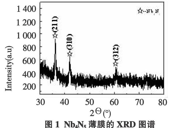
XRD testing was performed on the prepared Nb4N5 thin film, as shown in Figure 1. It can be seen that its XRD pattern is in 2 θ= The characteristic diffraction peaks of the Nb4N5 crystal appear at 36.1 °, 41.7 °, and 60.9 °, corresponding to the three crystal planes of the Nb4N5 crystal with a crystal surface index of (211), (220), and (312), respectively. The higher diffraction peak intensity in the pattern indicates that the crystallinity of Nb4N5 in the film is high, and the film phase is relatively pure, without other impurities.
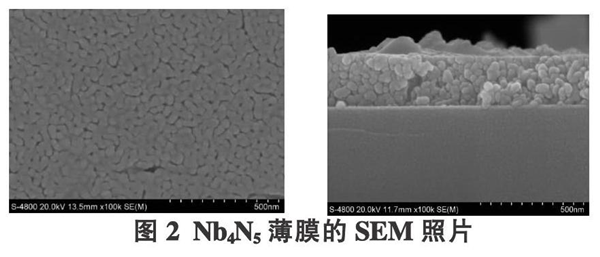
Figure 2 is a SEM photograph of the prepared Nb4N5 thin film. It can be seen that there are fewer surface cracks on the film, which are formed by the accumulation of many fine grains. The average grain size is 40 nm, and the thickness of the film is 210 nm. These Nb4N5 grains will form more SERS "hot spots", which helps to improve the SERS performance of the thin film. Due to the addition of PVP, it plays a role in preventing film cracking. During the drying and calcination process of the film, internal stress will be generated, resulting in film cracking. However, the addition of PVP can effectively alleviate the internal stress generated in the film and inhibit the formation of cracks. Polymer PVP is an organic polymer containing amino groups. It has a complex bipolar molecular structure. It contains both polar amino groups and non-polar methylene and methylene groups. In particular, the C=O contained in it can combine with hydroxyl groups or metal cations in the sol, making PVP molecules enter the gel film network structure, thus increasing the elasticity of the film. In addition, The decomposition of PVP at high temperatures can also cause structural relaxation of the film, thereby slowing down the formation of internal stress.
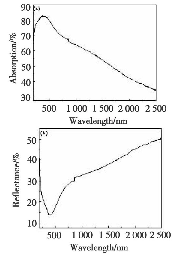
The absorbance, reflectivity, and transmittance of Nb4N5 thin film were tested in the ultraviolet visible near infrared range, and the results are shown in Figure 3 (a) - (c). In the absorption spectrum of the thin film, there is a plasmon resonance absorption peak in the range of 300 to 500 nm, which indicates that the electromagnetic field near the surface of the thin film increases under strong illumination, which will cause the polarization degree of molecules adsorbed near it to increase, resulting in surface enhanced Raman scattering performance. The transmittance of the thin film in the visible light range is low, but the reflectivity RIR in the infrared region is higher, greater than 30%. Through the four-probe tester test, it was found that the square resistance RS of the thin film is relatively small, with a resistance value of 552 Ω/□. This is mainly due to the relatively tight bonding of the thin film and the smooth surface of the thin film, which reduces the scattering of carriers. The reflectivity of the thin film is directly related to the square resistance. From the formula RIR=(1+0.0053RS) - 2, it can be seen that the smaller the square resistance, the greater the reflectivity of the thin film.
In order to test the SERS activity of the above Nb4N5 thin film, the thin film was immersed in 10-3M aqueous solution of R6G probe molecules for 5 minutes, and dried in air to conduct a SERS activity test. The results are shown in Figure 3 (d). The characteristic Raman vibration peak of R6G molecule can be seen in the Raman spectrum of the sample, wherein the Raman peak located at 620 cm-1 belongs to the C-C-C in-plane deformation vibration peak, the Raman peak located at 782 cm-1 corresponds to the C-H out-of-plane deformation vibration, the Raman peak located at 1187 cm-1 corresponds to the C-H and N-H bending vibration of the oxacene ring, and the Raman peaks located at 1360 cm-1 and 1656 cm-1 correspond to the C=C double bond stretching vibration of the oxacene ring. The peak strengths of the three peaks at Raman shifts of 620 cm-1, 782 cm-1, and 1656 cm-1 are 875 cps, 613 cps, and 909 cps, respectively. In contrast, when the concentration of R6G solution adsorbed on the quartz glass substrate is 10-3M, there is no obvious R6G Raman signal peak on its Raman spectrum, indicating that Nb4N5 thin film has good SERS activity, achieving Raman detection of R6G molecules. This is related to the surface plasmon resonance effect of niobium nitride on the one hand, and the narrow band gap of niobium nitride on the other hand. Molecules adsorbed on the surface of niobium nitride thin films can undergo charge transfer with them, and SERS activity can be achieved through chemical enhancement processes.
Conclusion
The Nb4N5 thin film prepared by the ammonia reduction nitridation method is relatively pure and has fewer cracks. It is formed by accumulation of grains, with an average particle diameter of 40 nm and a film thickness of 210 nm. Nb4N5 thin films exhibit excellent plasma absorption and infrared reflection characteristics, and have good SERS activity.
reference
[1] Wang Xiaohan, He Qianmei, Lu Zheng, et al. Effects of different sputtering conditions on the superconducting properties of ultra-thin epitaxial niobium nitride thin films [J]. Science Bulletin, 2019, 64 (20): 2127-2133
[2]KeskarK S, Yamashita T, Onodera Y, et al. rfreactively sputtered superconducting NbNx films[J]. Journal of Applied Physics,1974,45(7):3102-3105.
[3] Zhang Yijun, Zhang Xicheng, Luan Mingyu, et al. Study on the preparation and optical properties of NbSiN thin films [J]. Progress in Laser and Optoelectronics, 2017 (03): 316-322
[4]Naik G V, Shalaev V M, Boltasseva A. Alternative plasmonic materials: beyond gold and silver[J]. Advanced Materials,2013,25(24):3264-3294.
[5]Shen, H, Wei, B, Zhang, D, et al. Magnetron sputtered NbN thin film electrodes for supercapacitors[J]. Materials Letters,2018(229):17–20.
[6] Zhang Kan Study on the microstructure, mechanical properties, and tribological behavior of NbC and NbN based thin films [D]. Jilin University, 2014
[7]El-Shazly T S, Hassan W M, Rehim S S A E, et al. Optical and electronic properties of niobium oxynitrides with various N/O ratios: Insights from firstprinciples calculations[J]. Journal of Photonics for Energy,2018,8(2):1.
[8]S ysz W, Guziewicz M, Borysiewicz M, et al. Ultrathin NbN films for superconducting single-photon detectors[J]. Acta Physica Polonica A,2011,120(1):200-203.
[9] Song Jiaohua, Zhang Tao, Hou Junda, et al. Effect of deposition temperature on the microstructure of NbN films [J]. Journal of Beijing Normal University (Natural Science Edition), 2001 (1): 41-44
[10]Agnieszka W, Barbara K. XAFS investigations of nitrided NbN–SiO2 sol–gel derived films[J]. Journal of Non-Crystalline Solids,2012,358:969-974.
[11]Wei H, Wu M, Dong Z, et al. Composition, microstructure and SERS properties of titanium nitride thin film prepared via nitridation of sol–gel derived titania thin films[J]. Journal of Raman Spectroscopy, 2017,48(4):578-585.
[12] Feng Bokai, Fan Suhua, Zhang Fengqing, et al. Study on the preparation of ferroelectric ceramic thick films by the Sol-ge method [J]. Introduction to Materials, 2007021 (011): 25-29
[13] Wu Ling, Zhao Gaoling, Duan Gangfeng, et al. Structure and properties of V-doped TiN films at different deposition temperatures [J]. Functional Materials, 2011, 42 (4): 643-645
[14]CHENG C W, YAN B, WONG S M, et al. Fabrication and SERS performance of silver-nanoparticle-decorated Si/ZnO nanotrees in ordered arrays [J]. ACS Applied Materials & Interfaces,2010,2(7):1824-1828.