
Frontier hot spots! MXenes has six top issues a day, including AM, AEM, AFM, and Nano Letter
01
Ordered Design of Mo2Nb2C3Tx MXenes Atoms for Electrocatalysis of Hydrogen Evolution

The demand for new materials for energy storage and power generation requires chemical control at the atomic scale of nanomaterials. The discovery of ordered double transition metal MXenes in 2015 has expanded the chemical diversity of the atomic layered 2D material family. However, the atomic tunability of ordered MXenes to achieve ideal composition property relationships is not yet possible. In this study, we used density functional theory, Rietveld refinement, and electron microscopy methods to demonstrate Mo2+ α nb2− α Alc3 MAX phase (0 ≤ α≤ 0.3), and confirmed the prioritization behavior of Mo and Nb in the outer and inner M-layers, respectively. We also synthesized their two-dimensional derivative Mo2+ α Nb2− α C3Tx MXenes, and exemplified the effect of priority on their electrocatalytic behavior for hydrogen evolution reactions. The purpose of this study is to stimulate further exploration of the ordered double transition metal MXene family and contribute to the application driven design of two-dimensional materials by composing behavioral tools.
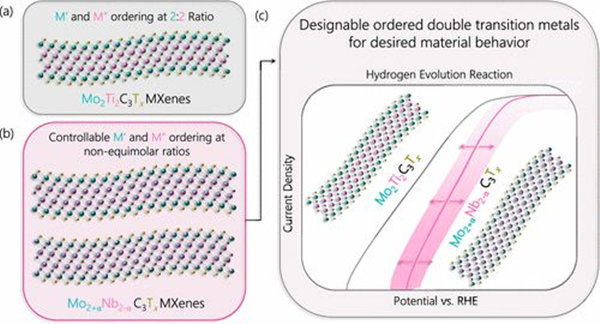
Ordered double transition metal Mo2+ α Nb2− α The application driven control of C3Tx provides control over the electrocatalytic HER behavior of MXenes. (a) The previous ordering of Mo2Ti2C3Tx MXenes was fixed, where the transition metal was separated into a separate layer of M atoms. (b) Mo2+ α Nb2− α C3Tx MXenes are orderly and controllable in the M-layer. (c) At Mo2+ α Nb2− α The controls obtained in C3Tx MXenes allow for designable material behavior, as shown in catalytic applications for hydrogen evolution reactions.
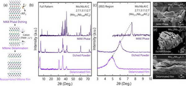
Etching and layering of Mo2 using HF-TMAOH method+ α Nb2− α Preparation of Mo2 from AlC3+ α Nb2− α C3Tx MXenes(a) Mo2+ α Nb2− α Generalized schematic diagram of etching, layering, and independent film preparation of C3Tx thin films. (b) Mo2+ α Nb2− α AlC3 MAX phase, etched Mo2+ α Nb2− α C3Tx MXene powder and independent Mo2+ α Nb2− α Full spectrum XRD of C3Tx delaminated MXene film (the actual composition in the arc is derived from Rietveld). (c) Full spectrum XRD focused on the (002) peak and found Mo2+ α Nb2− α AlC3 (002) peak shifts left to generate Mo2+ α Nb2− α C3Tx mxene (the actual composition of Rietveld is shown in parentheses). (d-f) Mo2+ α Nb2− α AlC3 MAX phase to Mo2+ α Nb2− α SEM images of C3Tx MXene independent films.
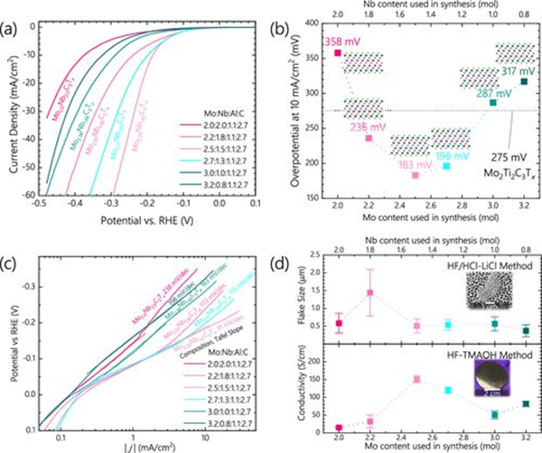
Synthesis of Mo2 from HF/hcl licl+ α Nb2− α Characterization of C3Tx MXenes by Hydrogen Evolution Reaction (HER) (a) Mo2+ α Nb2− α The potential and current density diagrams of C3Tx MXenes (the composition of Mo: Nb: Al: C in the figure, and the actual rietveld derived composition next to the data) are used to derive an overvoltage of 10 mA/cm2 and the Tafel slope shown in Figures (b) and (C), respectively. (d) HF tmao Synthetic Mo2+ α Nb2− α Conductivity measurement of C3Tx MXenes and Mo2 synthesized by HF/hcl licl+ α Nb2− α Comparison of sheet sizes for C3Tx MXenes.

The function and use of wearable triboelectric nano generators (TENGs) are significantly affected by the development of their friction material properties. A new type of charge generation layer (CGL) composed of V2CTx/organosilicon nanocomposites and S-TENG is introduced in this paper. The surface of V2CTx/silica gel nanocomposites exhibits high negative electricity, significantly increasing the surface potential and charge density. The peak power density of the prepared TENG is 19.75 W m − 2. It also exhibits high mechanical tensile properties (400%), which is significantly superior to the previously reported performance of TENGs under low external pressure. The optimized S-TENG is a self powered human motion sensor with high sensitivity (4.93 V kPa − 1) and fast rise time (21 ms). In addition, a realistic demonstration of sign language translation using finger motion detection and text conversion was successfully conducted through a smartphone. In addition, S-TENG's real-time sensing capabilities have been demonstrated in virtual reality car games controlled by finger touch. S-TENG has been proven to capture different types of human motion energy and continuously power stopwatches and wristwatches. Therefore, it is expected that V2CTx/silica gel nanocomposites will continue to contribute to various TENG applications, including wearable self powered sensors, robotics, and healthcare monitoring in Internet of Things platforms.
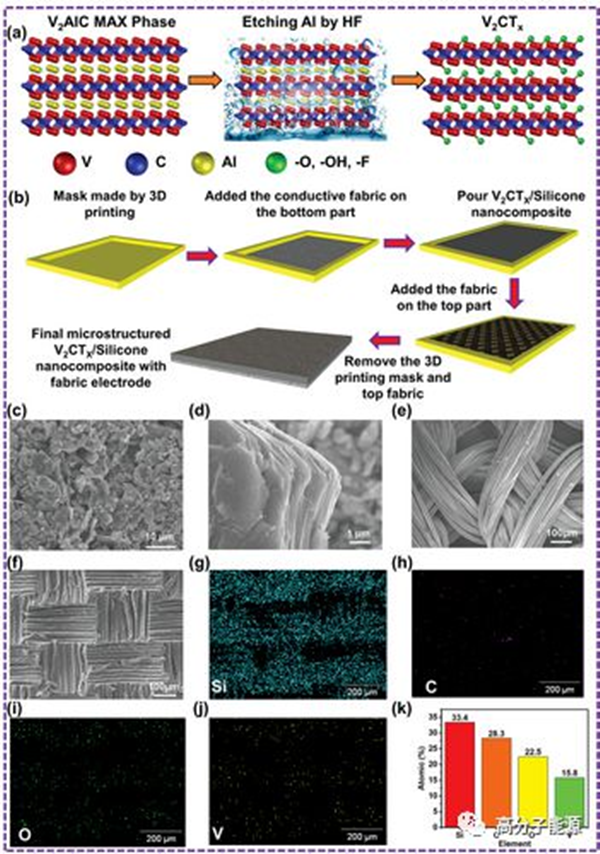
a) Schematic diagram of the selective etching procedure for V2AlC MAX level synthesis of V2CTx. b) A step by step preparation process for microstructure V2CTx/silicone nanocomposites. C-f) FESEM images of V2AlC Max phase particles, V2CTx MXene, nylon fabrics, and microstructure V2CTx/silica gel nanocomposites. G-k) EDS images and corresponding element diagrams.
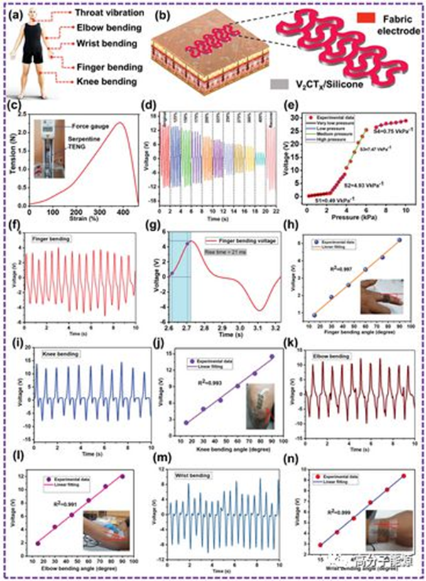
a) The proposed S-TENG diagram illustrates the human body position for motion sensors. b) Schematic diagram of S-TENG attached to the skin and an enlarged image of S-TENG. c) Tension strain curve of S-TENG (dynamometer attached to S-TENG diagram). d) The voltage output performance of the S-TENG sensor at different strain levels. e) The S-TENG output voltage and pressure sensitivity depend on the range of applied pressure. f) The voltage signal generated by the S-TENG sensor when the finger is bent. g) The rise time of the S-TENG sensor to bend and release the finger. i. K, m) Response of S-TENG output voltage signals to knee, elbow, and wrist flexion relative to different angles. h. J, l, n) At a certain bending angle, the output S-TENG voltage linearly increases with the increase in the bending degree of the fingers, knees, elbows, and wrists.

a) The voltage signal of the S-TENG sensor when the throat vibrates (in the image: sensor image, fixed to the human throat). When a person's throat vibrates, the voltage signals emitted by the S-TENG sensor are identified as b) "Hi," "Sanaf," "I love you," and c) "How are you?" d) Photos of five S-TENG sensors mounted on their fingers. e) The S-TENG sensor responds to voltage signals from various finger movements. f) The sign language of "HELLO ASER" is represented by a color map of the output voltage of each S-TENG sensor. g) Schematic diagram of the architecture of the sign language translation system. h) Photos of S-TENG and smartphone apps show gestures for text translation. i) Schematic diagram of two-dimensional car game control scheme (sensor array, data acquisition scheme, Bluetooth, MCU, game interface computer) j, k) Photos of S-TENG sensor array and game interface PC. l) Using the S-TENG array, by manually tapping, it was demonstrated that there were 33 μ F and 10 μ Self powered wrist watch and stopwatch with F voltage curve.
03
Construction of Flexible Thin Film Electrode with Porous Layered Structure Using MXene/SWCNTs/PANI Ternary Composite Materials
Among the energy lost due to various inefficiencies, thermal energy is abundant and widespread. Using the thermoelectric effect, thermal batteries (TECs) can directly convert thermal energy into electrical energy without generating vibration, noise, or other waste emissions. This paper proposes a reasonable design of a flexible thin film electrode based on the ternary composite material Ti3C2Tx MXene (Tx represents the surface end), polyaniline (PANI), and single walled carbon nanotubes. Compared with the widely used platinum electrode, the thermoelectric chemical properties of this electrode are significantly improved. The ternary composite electrode forms a porous layered structure with a large electrochemical active surface area. Experimental and simulation results show that the synergistic effect of Ti3C2Tx and PANI promotes mass and charge transfer at the electrolyte electrode interface Δ An output power of 13.15 is generated at a T of 40 K μ TEC of W cm − 2. TEC has also shown a rapid response to the small temperature differences between the human body and the environment, demonstrating great potential in collecting low-level heat to power small electronic devices.
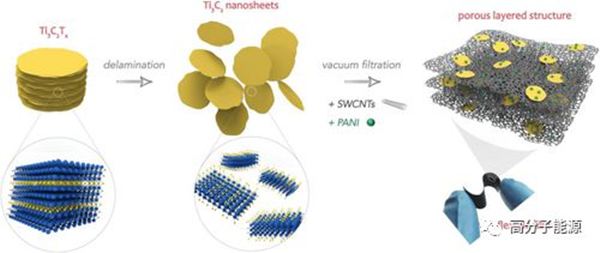
Formation of porous layered ternary composite thin film electrodes.
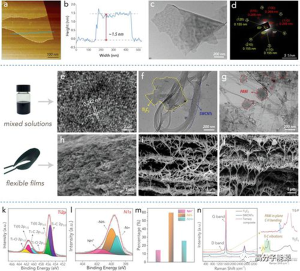
a) Synthetic AFM images of Ti3C2Tx MXene wafers. b) An AFM height profile of a synthetic Ti3C2Tx MXene sheet. c) TEM image of the original Ti3C2Tx sheet. d) The selected region electron diffraction (SAED) pattern corresponding to the original Ti3C2Tx (P63/mmc space group, No. 194). e) High resolution TEM images obtained by mixing Ti3C2Tx with SWCNTs and PANI. f) Transmission electron microscope images of Ti3C2Tx+SWCNTs binary composites. g) TEM images of Ti3C2Tx+SWCNTs+PANI ternary composites. h) SEM cross-sectional view of the original Ti3C2Tx film. i) SEM cross-sectional images of Ti3C2Tx+SWCNTs binary composite films. j) SEM cross-sectional view of Ti3C2Tx+SWCNTs+PANI ternary composite film. k) XPS Ti2p spectra of Ti3C2Tx+SWCNTs+PANI ternary composites. l) XPS N1s spectra of Ti3C2Tx+SWCNTs+PANI ternary composites. m) The integral area of the three subpeaks of the deconvolution of the N1s spectrum. n) Raman spectra of various samples.
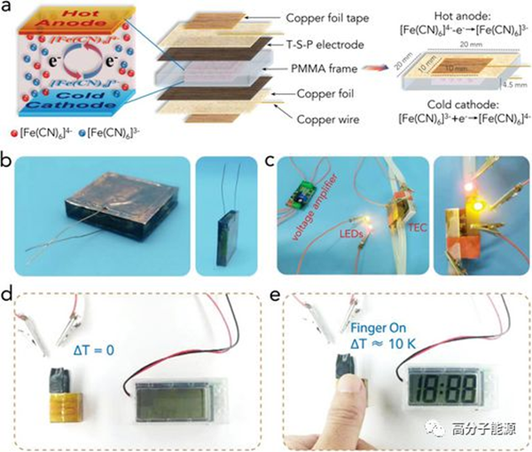
a) Schematic diagram of square TEC structure and size information. b) Prefabricate an optical image of a square TEC. c) Demonstration of lighting two LED bulbs using a square TEC assisted by a voltage amplifier at a temperature difference of 30 K. d. E) Demonstrate using a square TEC to power an electronic timer by collecting human body heat. The timer starts immediately when the thumb touches one side of the square TEC. The applied temperature difference between the human body and the surrounding environment is ≈ 10 K.
In lithium sulfur batteries, it is significant but challenging to prepare metal boride heterostructures and decipher their interfacial interaction mechanisms that accelerate the conversion of polysulfides at the atomic level. Here, a novel high conductivity and binary thiophilic NbB2 MXene heterostructure with a spontaneous built-in electric field (BIEF) has been carefully designed through a simple one-step boron thermal reduction strategy. Experimental and theoretical results show that Nb and B atoms can form chemical bonds with polysulfides, enriching chemical anchor points and catalytic active sites. At the same time, spontaneous BIEF induces interfacial charge redistribution, causing more electrons to transfer to the NbB2 surface site, thereby weakening its strong adsorption performance. However, it accelerates the transfer and electron diffusion of polysulfides at the heterogeneous interface, providing a moderate polysulfide adsorption capacity, but reducing the sulfur conversion barrier, further enhancing the intrinsic catalytic activity of NbB2 mxene to accelerate bidirectional sulfur conversion. Therefore, the S/NbB2 MXene cathode has a high initial capacity of 1310.1 mAh g − 1 at 0.1 ℃, a stable long-term service life of 500 times at 1 ℃ (capacity attenuation per cycle of 0.076%), and a large area capacity of 6.5 mAh cm − 2 at 0.1 ℃ (at 5 μ The sulfur load in a dilute electrolyte of L mg − 1 is 7.0 mg cm − 2). This work clearly reveals the mechanism of interface BIEF and binary sulfonation effect accelerating sulfur conversion at the atomic level.
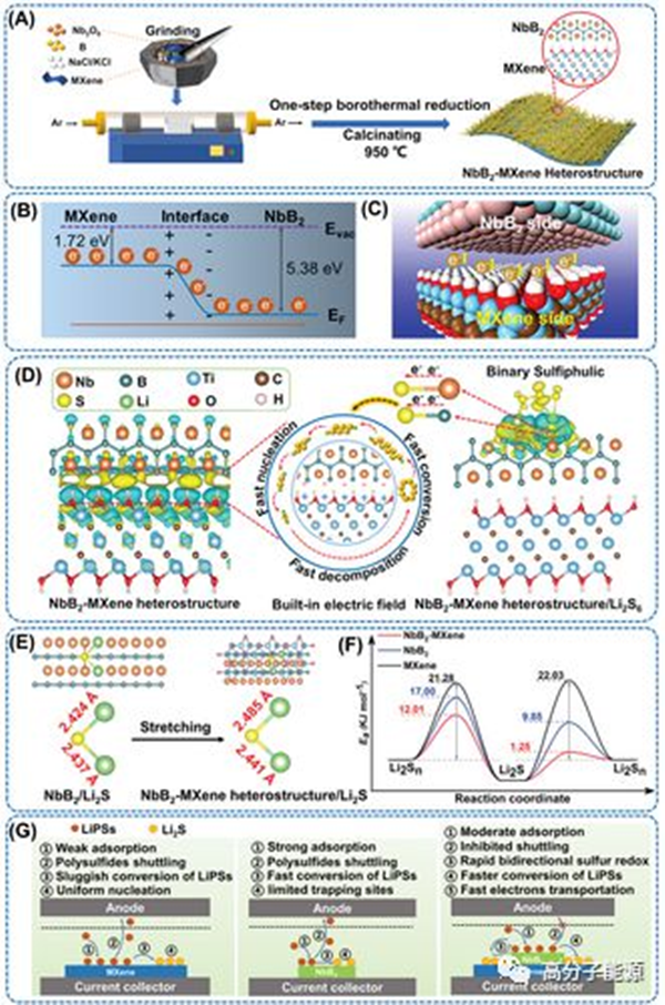
Synthesis process and mechanism of NbB2 MXene heterostructures. A) Synthesis scheme of NbB2 MXene heterostructure. B. C) Schematic diagram of electron redistribution on the NbB2 and MXene interfaces. D) The interfacial charge density difference between NbB2 and MXene and the adsorption electrocatalytic mechanism of NbB2 MXene heterostructures on LiPSs. The yellow and blue distributions represent the accumulation and consumption of electric charges, respectively. E) Schematic diagram of Li2S adsorption on NbB2 and NbB2 mxene surfaces and Li × The key length of the S key. F) Conversion activation energy of polysulfides/Li2S on MXene, NbB2, and NbB2-MXene. G) Schematic diagram of polysulfide adsorption/conversion processes on the surfaces of NbB2, MXene, and NbB2 MXene, respectively.
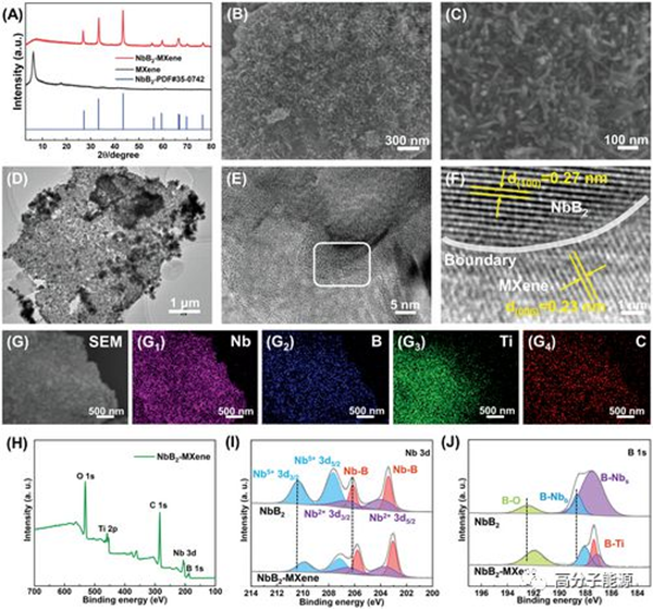
Morphology and microstructure of NbB2 MXene heterostructures. A) XRD spectrogram. B. C) NbB2 MXene of SEM and D) TEM images. E. F) HR-TEM image of NbB2-MXene. G) Element mapping of SEM images and their Nb, B, Ti, and C (G1-G4). H) XPS spectroscopic determination of NbB2 MXene. High resolution XPS spectra of NbB2 MXene for I) Nb 3d and J) B 1s.

Electrocatalytic hydrogen evolution (HER) in mild neutral media is an important goal for environmentally sustainable energy conversion, but its development is greatly limited due to its slow kinetics. Platinum group precious metals have extremely high HER activity, but their scarcity and performance instability limit their wide application. Here, utilizing the excellent catalyst support properties of 2d layered transition metal carbides (MXene), the highly dispersed Ru clusters on Mo2CTx MXene have been proven to be an excellent HER electrocatalyst prepared using an in situ reduction strategy. The prepared Ru/Mo2CTx catalyst exhibits an over potential of 73 mV in neutral media, reaching a current density of − 10 mA cm − 2 and a Tafel slope of 57 mV dec − 1, surpassing the performance of most mxenen-based catalysts previously reported. In addition, the stability of Ru/Mo2CTx catalysts is also better than commercial Pt/C catalysts. Experimental results and theoretical calculations indicate that the interaction between Ru clusters regulates the electronic structure of the active sites, promoting the dissociation of water and the desorption of hydrogen.
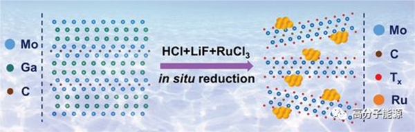
Schematic diagram of a simple synthesis of Ru/Mo2CTx from Mo2Ga2C.
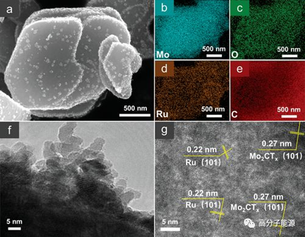
Characterization of the microstructure and morphology of Ru/Mo2CTx. a) SEM images with uniform distribution of Ru clusters; B-e) EDX element mapping; F-g) HR-TEM images.
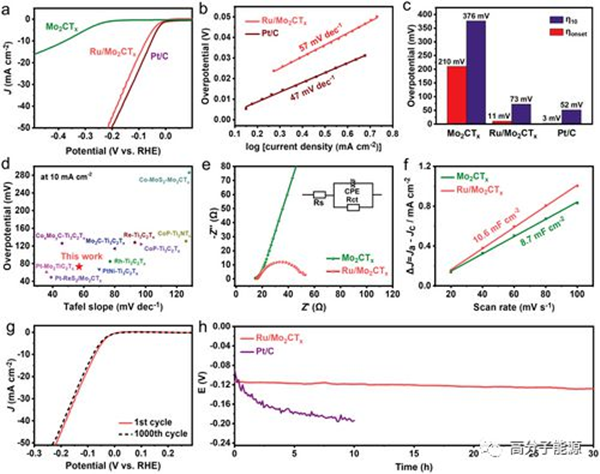
Electrochemical HER performance in neutral media. a) HER polarization curve at a scanning rate of 5 mV s − 1; b) Tafel diagram derived from part (a); c) The initial potential and overvoltage of Mo2CTx, Ru/Mo2CTx, and Pt/c at − 10 mA cm − 2; d) Comparison of overvoltage and Tafel slope of various mxene based HER catalysts; e) Nyquist diagram of electrochemical impedance spectroscopy; f) Linear fitting of capacitive current and CV scanning rate; g) Stability demonstration after 1 and 1000 cycles of Ru/Mo2CTx; h) Demonstration of chronopotentiometric stability of Ru/Mo2CTx at − 20 mA cm − 2 for 30 hours.
06
Controllable distribution of Ti3C2Tx hollow microspheres on thermally conductive polyimide films for excellent electromagnetic interference shielding
Flexible multifunctional polymer based electromagnetic interference shielding composite films have important applications in 5G communication technology, wearable electronic devices, artificial intelligence, and other fields. Based on the porous/multilayer structure design, a flexible (Fe3O4/PI) - Ti3C2Tx - (Fe3O4/PI) composite film with controllable pore size and distribution was successfully prepared using a sacrificial template method using polyimide (PI) as the matrix and polymethyl methacrylate (PMMA) microspheres as the template. Due to the porous/multilayer structure of Ti3C2Tx hollow microspheres, when the pore diameter is 10 μ m. When the PMMA/Ti3C2Tx mass ratio is 2:1, the EMI shielding performance of (Fe3O4/PI) - Ti3C2Tx - (Fe3O4/PI) composite film is the most excellent, with an EMI shielding effectiveness (EMI SE) of 85 dB. Through finite element simulation, it is further verified that the composite film has a good shielding effect on electromagnetic waves. In addition, the composite film has good thermal conductivity (thermal conductivity of 3.49 W/(m · K)) and mechanical properties (tensile strength of 65.3 MPa). This flexible (Fe3O4/PI) - ti3c2tx - (Fe3O4/PI) composite film has excellent EMI shielding performance, thermal conductivity, and mechanical properties, showing great application potential in the EMI shielding protection of high-power, portable, and wearable flexible electronic devices.
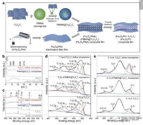
a) Schematic diagram for the preparation of (Fe3O4/PI) - ti3c2tx - (Fe3O4/PI) composite thin films. PMMA microspheres, Ti3C2Tx PMMA@Ti3C2Txmicrosphere Characterization results of ti3c2tx hollow microspheres: b) XRD spectrum, c) XPS full spectrum, and d) high-resolution XPS narrow spectrum of ti2cpand e) c1s
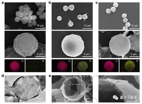
PMMA microspheres PMMA@Ti3C2Txmicrospheres Morphology of Ti3C2Txhole microspheres: a) PMMA microspheres, b) PMMA@Ti3C2Txmicrospheres And C) SEM images of C and Ti elements and corresponding EDS element distribution diagrams of Ti3C2Txhole microspheres; d) Transmission electron microscope images of ti3c2tx hollow microspheres; e) SEM images of deliberately crushed ti3c2tx hollow microspheres were observed for wall thickness.
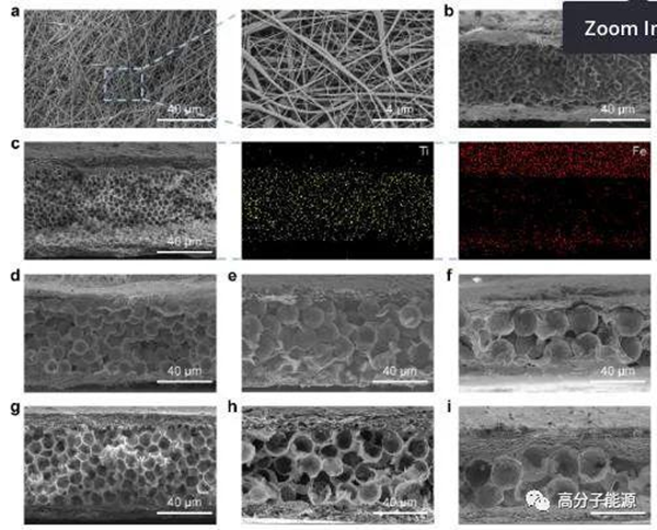
Fe3O4/PAA electrospinned nanofiber films with different diameters (Fe3O4/PI)- PMMA@Ti3C2Tx -Morphology of (Fe3O4/PI) composite films and corresponding (Fe3O4/PI) - ti3c2tx - (Fe3O4/PI) composite films: a) SEM images of the surface of Fe3O4/PAA electrospinned nanofibers. All rights reserved. 14 Movies; b) Diameter 5 μ And c) (Fe3O4/PI)- PMMA@Ti3C2Tx -SEM cross-sectional view of (Fe3O4/PI) composite film (with EDS element distribution diagram of Fe and Ti elements attached); d-f)、(Fe3O4/PI) - PMMA@Ti3C2Tx -(Fe3O4/PI) with a diameter of 10 respectively μ m、15 μ M and 20 μ Cross-sectional sem images of (Fe3O4/PI) - ti3c2tx - (Fe3O4/PI) composite films corresponding to g-i
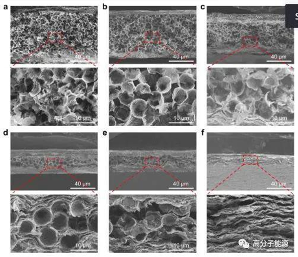
Morphology of (Fe3O4/PI) - Ti3C2Tx - (Fe3O4/PI) composite films based on different mass ratios of PMMA/Ti3C2Tx: SEM cross-sectional view of (Fe3O4/PI) - Ti3C2Tx - (Fe3O4/PI) composite films prepared with PMMA/Ti3C2Tx mass ratios of a) 4:1, b) 2:1, c) 1:1, d) 1:2, e) 1:4, and f) 0:1.
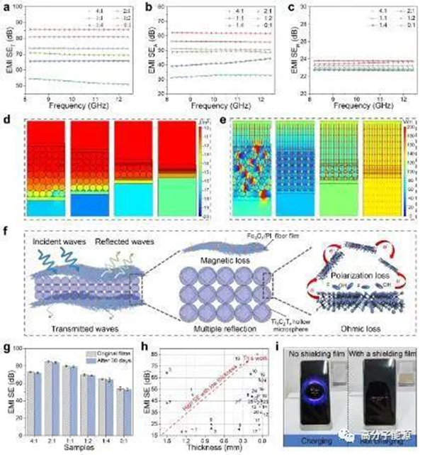
Non PMMA/Ti3C2TX quality hoe (Fe3O4/PI) - Ti3C2TX - (Fe3O4/PI) reply; d) PMMA/Ti3c2tx4:1, 2:1, 1:2, 0:1 blanking (Fe3O4/PI) - Ti3c2tx - (Fe3O4/PI) reply; e) Electricity; f) Figure; g) (Fe3O4/PI) - Ti3C2Tx - (Fe3O4/PI) reply; h) (fe3o4/pi) - ti3c2tx - (fe3o4/pi) reply; i) Display time and time interval (Fe3O4/PI) - Ti3C2Tx - (Fe3O4/PI) replication